Our layers are fabricated on a Magnetron Sputter Deposition Equipment (MSD) and an Ion Beam Sputter Deposition Tool (IBSD) which allow the production of very smooth and uniform layers. In addition, based on a superior substrate positioning system we are capable to deposit very precisely multilayer gradients across the substrate as well as depth graded multilayers to provide sophisticated X-ray optics addressing customer’s needs.
Deposition

Deposition Tools
MSD
Magnetron sputtering with noble gas is a well-established technique that has been used for many decades in the area of X-ray multilayer fabrication. Due to the magnetic field a dense plasma close to the sputter target surface can be sustained even for typically low process pressure below 1×10⁻³ mbar which yields to relatively high deposition rates around 1 nm/s and a high mean free path of film forming species at the same time. This supports the formation of high-quality thin films as it enables to synthesize dense layers with relatively smooth interfaces between absorber and spacer in the order of ~0.3 nm. Both is a major prerequisite to yield high multilayer reflectivities. Our DC magnetron sputter tool is equipped with four radially arranged planar magnetrons with a size of 300 mm, thus any supportive adhesion layer respective cover layer can be applied without any contact to ambient air. During the fabrication process the substrate orbitally rotates above the magnetrons and optionally can spin around its own axis in order to allow the formation of extremely uniform layers.
IBSD
Sputter ion generation takes place by Electron Cyclotron Resonance (ECR) activation of a noble gas (Argon or Krypton) in a linear plasma source across a length of 400 mm. Subsequently an ion beam is extracted by a grid system and focused onto the target with an adjustable energy of the sputter ions in the range of 100 eV to 1500 eV. Up to 6 different target materials can be placed on a rotatable target revolver which is a prerequisite for multilayer synthesis. The film forming species in ion beam sputter process are typically higher energetic compared to those present in magnetron sputtering processes. Combined with a lower process pressure in the range of 10-4 mbar ion beam sputtering yields layers with reduced surface roughness, high material density and low defect numbers. The substrate is moved linearly across differently shaped slits and if required it can be rotated during the deposition process. Thus, a substrate size with a diameter up to 200 mm and linear substrates up to 500 mm can be coated.
A secondary ion beam source provides additional features:
- Ion beam cleaning
- Ion beam smoothing
- Ion beam etching
- Ion beam figuring
- Ion beam enhancement
Specifications
Deposition elements (others on request):
Ag, Al, Au, B4C, C, Cr, Cu, Fe, Ir, La, Mn, Mo, MoSi2, Ni, NiV, Pd, Ru, Sc, Si, SiC, Ta, Ti, V, W, WSi2, Zr
Multilayer systems (others on request):
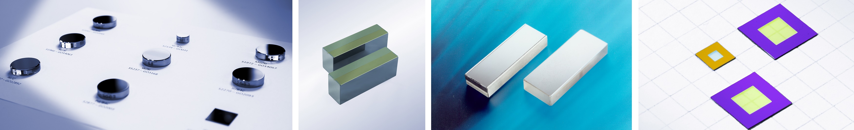
W/Si, WSi2/Si, W/B4C, Mo/Si, MoSi2/Si, Mo/B4C, Ni/C, Ni/B4C, Cr/C, Cr/Sc, La/B4C, Pd/B4C, Ru/C, Ru/B4C, Si/B4C
Dimensions:
diameter up to 200 mm or length up to 500 mm (depending on coating type)
Applications
Coating applications
MSD and IBSD coatings can be used for countless applications in industrial and R&D environments. A selection of coatings made by AXO DRESDEN is shown below:
- Multilayers for X-ray fluorescence (XRF) analysis
- Göbel mirrors for X-ray diffraction (XRD)
- Teaching tools for X-ray reflectometry (XRR)
- Synchrotron optics based on total reflection coatings or multilayer monochromator stacks
- Tailored 2D collimating or focussing optics for microfocus, rotating anode or MetalJet sources
- Monochromators and optics from EUV to the hard X-ray regime
- Thin film XRF reference samples on wafers, foils and Si3N4 membranes
- Sub-nanometer TXRF reference samples
- Coatings of optical gratings from EUV to hard X-rays
Characterization
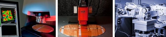
XRD
One fundamental characterization method for all depositions used in X-ray applications is X-ray diffractometry. A θ-2θ scan (X-ray reflectometry, XRR) is performed in a Cu-Kα twin mirror arrangement in order to determine its reflectivity and bandwidth. Based on the reflectivity curve by means of XRR simulation one can retrieve several important layer characteristics such as density of absorber and spacer, interface roughness in combination with interdiffusion at the interface, as well as period thickness ratio Γ.
AFM
An Atomic Force Microscope (Nanosurf Nanite) is utilized to characterize substrate roughness as well as the surface topography of deposited layers in the high spatial frequency range. In terms of total reflection and high order Bragg reflection performance it is a crucial information on which the improvement of all deposition processes takes place. Any accumulation of roughness during the multilayer formation has to be avoided respectively minimized. On the other hand, especially for high resolution multilayers extremely smooth substrates are essential and by means of AFM characterization quality control is provided in advance of the deposition process. Typically, the substrate roughness of X-ray optics is in the order of 0.1-0.15 nm rms.
WLI
Besides high spatial frequency information of an optical system which is determined by the multilayer and the polishing quality of the used substrate surface another characteristic is its slope error. Usually this information is gained in the mid spatial frequency range by white light interferometry measurements (ZYGO Nexview). In Addition, WLI is well suited to visualize any undesired defects like bumps, droplets or scratches.